Monday, August 31, 2015

The PN Junction Diode

The effect described in the previous tutorial is achieved without any external voltage being applied to the actual PN junction resulting in the junction being in a state of equilibrium. However, if we were to make electrical connections at the ends of both the N-type and the P-type materials and then connect them to a battery source, an additional energy source now exists to overcome the potential barrier.
The effect of adding this additional energy source results in the free electrons being able to cross the depletion region from one side to the other. The behaviour of the PN junction with regards to the potential barrier’s width produces an asymmetrical conducting two terminal device, better known as the PN Junction Diode.
A PN Junction Diode is one of the simplest Semiconductor Devices around, and which has the characteristic of passing current in only one direction only. However, unlike a resistor, a diode does not behave linearly with respect to the applied voltage as the diode has an exponential current-voltage ( I-V ) relationship and therefore we can not described its operation by simply using an equation such as Ohm’s law.
If a suitable positive voltage (forward bias) is applied between the two ends of the PN junction, it can supply free electrons and holes with the extra energy they require to cross the junction as the width of the depletion layer around the PN junction is decreased.
By applying a negative voltage (reverse bias) results in the free charges being pulled away from the junction resulting in the depletion layer width being increased. This has the effect of increasing or decreasing the effective resistance of the junction itself allowing or blocking current flow through the diode.
Then the depletion layer widens with an increase in the application of a reverse voltage and narrows with an increase in the application of a forward voltage. This is due to the differences in the electrical properties on the two sides of the PN junction resulting in physical changes taking place. One of the results produces rectification as seen in the PN junction diodes static I-V (current-voltage) characteristics. Rectification is shown by an asymmetrical current flow when the polarity of bias voltage is altered as shown below.

Junction Diode Symbol and Static I-V Characteristics.

pn junction diode characteristics
But before we can use the PN junction as a practical device or as a rectifying device we need to firstly bias the junction, ie connect a voltage potential across it. On the voltage axis above, “Reverse Bias” refers to an external voltage potential which increases the potential barrier. An external voltage which decreases the potential barrier is said to act in the “Forward Bias” direction.
There are two operating regions and three possible “biasing” conditions for the standard Junction Diode and these are:
  • 1. Zero Bias – No external voltage potential is applied to the PN junction diode.
  • 2. Reverse Bias – The voltage potential is connected negative, (-ve) to the P-type material and positive, (+ve) to the N-type material across the diode which has the effect of Increasing the PN junction diode’s width.
  • 3. Forward Bias – The voltage potential is connected positive, (+ve) to the P-type material and negative, (-ve) to the N-type material across the diode which has the effect of Decreasing the PN junction diodes width.

Zero Biased Junction Diode

When a diode is connected in a Zero Bias condition, no external potential energy is applied to the PN junction. However if the diodes terminals are shorted together, a few holes (majority carriers) in the P-type material with enough energy to overcome the potential barrier will move across the junction against this barrier potential. This is known as the “Forward Current” and is referenced as IF
Likewise, holes generated in the N-type material (minority carriers), find this situation favourable and move across the junction in the opposite direction. This is known as the “Reverse Current” and is referenced as IR. This transfer of electrons and holes back and forth across the PN junction is known as diffusion, as shown below.

Zero Biased PN Junction Diode

pn junction zero bias
The potential barrier that now exists discourages the diffusion of any more majority carriers across the junction. However, the potential barrier helps minority carriers (few free electrons in the P-region and few holes in the N-region) to drift across the junction.
Then an “Equilibrium” or balance will be established when the majority carriers are equal and both moving in opposite directions, so that the net result is zero current flowing in the circuit. When this occurs the junction is said to be in a state of “Dynamic Equilibrium“.
The minority carriers are constantly generated due to thermal energy so this state of equilibrium can be broken by raising the temperature of the PN junction causing an increase in the generation of minority carriers, thereby resulting in an increase in leakage current but an electric current cannot flow since no circuit has been connected to the PN junction.

Reverse Biased PN Junction Diode

When a diode is connected in a Reverse Bias condition, a positive voltage is applied to the N-type material and a negative voltage is applied to the P-type material.
The positive voltage applied to the N-type material attracts electrons towards the positive electrode and away from the junction, while the holes in the P-type end are also attracted away from the junction towards the negative electrode.
The net result is that the depletion layer grows wider due to a lack of electrons and holes and presents a high impedance path, almost an insulator. The result is that a high potential barrier is created thus preventing current from flowing through the semiconductor material.

Increase in the Depletion Layer due to Reverse Bias

pn junction reverse bias
This condition represents a high resistance value to the PN junction and practically zero current flows through the junction diode with an increase in bias voltage. However, a very small leakage current does flow through the junction which can be measured in micro-amperes, ( μA ).
One final point, if the reverse bias voltage Vr applied to the diode is increased to a sufficiently high enough value, it will cause the diode’s PN junction to overheat and fail due to the avalanche effect around the junction. This may cause the diode to become shorted and will result in the flow of maximum circuit current, and this shown as a step downward slope in the reverse static characteristics curve below.

Reverse Characteristics Curve for a Junction Diode

pn junction diode reverse characteristics
Sometimes this avalanche effect has practical applications in voltage stabilising circuits where a series limiting resistor is used with the diode to limit this reverse breakdown current to a preset maximum value thereby producing a fixed voltage output across the diode. These types of diodes are commonly known as Zener Diodes and are discussed in a later tutorial.

Forward Biased PN Junction Diode

When a diode is connected in a Forward Bias condition, a negative voltage is applied to the N-type material and a positive voltage is applied to the P-type material. If this external voltage becomes greater than the value of the potential barrier, approx. 0.7 volts for silicon and 0.3 volts for germanium, the potential barriers opposition will be overcome and current will start to flow.
This is because the negative voltage pushes or repels electrons towards the junction giving them the energy to cross over and combine with the holes being pushed in the opposite direction towards the junction by the positive voltage. This results in a characteristics curve of zero current flowing up to this voltage point, called the “knee” on the static curves and then a high current flow through the diode with little increase in the external voltage as shown below.

Forward Characteristics Curve for a Junction Diode

pn junction forward characteristics
The application of a forward biasing voltage on the junction diode results in the depletion layer becoming very thin and narrow which represents a low impedance path through the junction thereby allowing high currents to flow. The point at which this sudden increase in current takes place is represented on the static I-V characteristics curve above as the “knee” point.

Reduction in the Depletion Layer due to Forward Bias

pn junction forward bias
This condition represents the low resistance path through the PN junction allowing very large currents to flow through the diode with only a small increase in bias voltage. The actual potential difference across the junction or diode is kept constant by the action of the depletion layer at approximately 0.3v for germanium and approximately 0.7v for silicon junction diodes.
Since the diode can conduct “infinite” current above this knee point as it effectively becomes a short circuit, therefore resistors are used in series with the diode to limit its current flow. Exceeding its maximum forward current specification causes the device to dissipate more power in the form of heat than it was designed for resulting in a very quick failure of the device.

Junction Diode Summary

The PN junction region of a Junction Diode has the following important characteristics:
  • Semiconductors contain two types of mobile charge carriers, Holes and Electrons.
  • The holes are positively charged while the electrons negatively charged.
  • A semiconductor may be doped with donor impurities such as Antimony (N-type doping), so that it contains mobile charges which are primarily electrons.
  • A semiconductor may be doped with acceptor impurities such as Boron (P-type doping), so that it contains mobile charges which are mainly holes.
  • The junction region itself has no charge carriers and is known as the depletion region.
  • The junction (depletion) region has a physical thickness that varies with the applied voltage.
  • When a diode is Zero Biased no external energy source is applied and a natural Potential Barrier is developed across a depletion layer which is approximately 0.5 to 0.7v for silicon diodes and approximately 0.3 of a volt for germanium diodes.
  • When a junction diode is Forward Biased the thickness of the depletion region reduces and the diode acts like a short circuit allowing full current to flow.
  • When a junction diode is Reverse Biased the thickness of the depletion region increases and the diode acts like an open circuit blocking any current flow, (only a very small leakage current).
We have also seen above that the diode is two terminal non-linear device whose I-V characteristic are polarity dependent as depending upon the polarity of the applied voltage, VD the diode is either Forward Biased, VD > 0 or Reverse Biased, VD < 0. Either way we can model these current-voltage characteristics for both an ideal diode and for a real diode.

Junction Diode Ideal and Real Characteristics

junction diode ideal and real characteristics
In the next tutorial about diodes, we will look at the small signal diode sometimes called a switching diode which is used in general electronic circuits. As its name implies, the signal diode is designed for low-voltage or high frequency signal applications such as in radio or digital switching circuits.
Signal diodes, such as the 1N4148 only pass very small electrical currents as opposed to the high-current mains rectification diodes in which silicon diodes are usually used. Also in the next tutorial we will examine the Signal Diode static current-voltage characteristics curve and parameters.

Normal Diodes

Standard signal diodes are among the most basic, average, no-frills members of the diode family. They usually have a medium-high forward voltage drop and a low maximum current rating. A common example of a signal diode is the 1N4148. Very general purpose, it’s got a typical forward voltage drop of 0.72V and a 300mA maximum forward current rating.
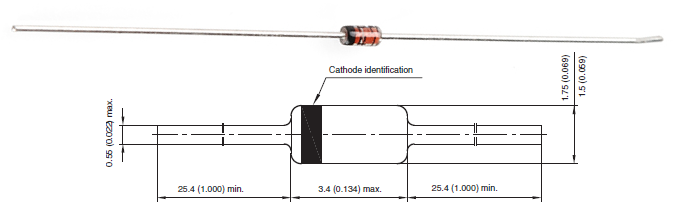
1N4148 image plus a mechanical drawing
A small-signal diode, the 1N4148. Notice the black circle around the diode, that marks which of the terminals is the cathode.
A rectifier or power diode is a standard diode with a much higher maximum current rating. This higher current rating usually comes at the cost of a larger forward voltage. The 1N4001, for example, has a current rating of 1A and a forward voltage of 1.1V.
1N4001 image
A 1N4001 PTH diode. This time a gray band indicates which pin is the cathode.
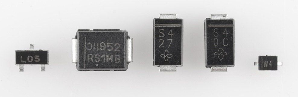
And, of course, most diode types come in surface-mount varieties as well. You’ll notice that every diode has some way (no matter how tiny or hard to see) to indicate which of the two pins is the cathode.
Some SMD diodes

Light-Emitting Diodes (LEDs!)

The flashiest member of the diode family must be the light-emitting diode (LED). These diodes quite literally light up when a positive voltage is applied.
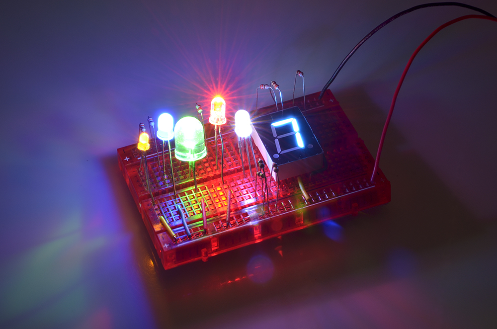
Examples of LEDs
A handful of through-hole LEDs. From left to right: a yellow 3mm, blue 5mm, green 10mm, super-bright red 5mm, an RGB 5mm and a blue 7-segment LED.
Like normal diodes, LEDs only allow current through one direction. They also have a forward voltage rating, which is the voltage required for them to light up. The VF rating of an LED is usually larger than that of a normal diode (1.2~3V), and it depends on the color the LED emits. For example, the rated forward voltage of a Super Bright Blue LED is around 3.3V, while that of the equal size Super Bright Red LED is only 2.2V.
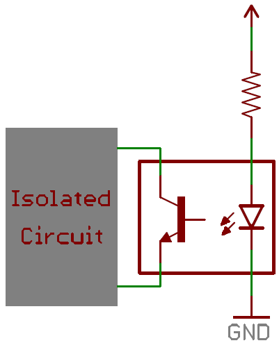
You’ll obviously most-often find LEDs in lighting applications. They’re blinky and fun! But more than that, their high-efficiency has lead to widespread use in street lights, displays, backlighting, and much more. Other LEDs emit a light that is not visible to the human eye, like infrared LEDs, which are the backbone of most remote controls. Another common use of LEDs is in optically isolating a dangerous high-voltage system from a lower-voltage circuit. Opto-isolators pair an infrared LED with a photosensor, which allows current to flow when it detects light from the LED. Below is an example circuit of an opto-isolator. Note how the schematic symbol for the diode varies from the normal diode. LED symbols add a couple arrows extending out from the symbol.
LED in an opto-isolator circuit

Schottky Diodes

Another very common diode is the Schottky diode. The semiconductor composition of a Schottky diode is slightly different from a normal diode, and this results in a much smaller forward voltage drop, which is usually between 0.15V and 0.45V. They’ll still have a very large breakdown voltage though.
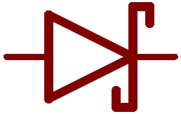
Schottky diodes are especially useful in limiting losses, when every last bit of voltage must be spared. They’re unique enough to get a circuit symbol of their own, with a couple bends on the end of the cathode-line.
Schottky diode circuit symbol

Zener Diodes

Zener diodes are the weird outcast of the diode family. They’re usually used to intentionally conduct reverse current. Zener’s are designed to have a very precise breakdown voltage, called the zener breakdown or zener voltage. When enough current runs in reverse through the zener, the voltage drop across it will hold steady at the breakdown voltage.
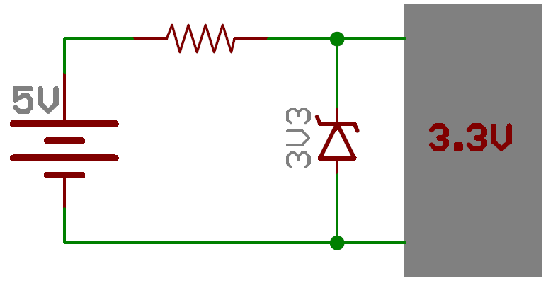
Taking advantage of their breakdown property, Zener diodes are often used to create a known reference voltage at exactly their Zener voltage. They can be used as a voltage regulator for small loads, but they’re not really made to regulate voltage to circuits that will pull significant amounts of current.
Zeners are special enough to get their own circuit symbol, with wavy ends on the cathode-line. The symbol might even define what, exactly, the diode’s zener voltage is. Here’s a 3.3V zener diode acting to create a solid 3.3V voltage reference:
Zener 3.3V reference circuit

Photodiodes

Photodiodes are specially constructed diodes, which capture energy from photons of light (see Physics, quantum) to generate electrical current. Kind of operating as an anti-LED.
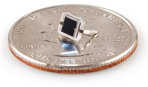
BPW34 Photodiode
A BPW34 photodiode (not the quarter, the little thing on top of that). Get it under the sun and it can generate about few µW’s of power!.
Solar cells are the main benefactor of photodiode technology. But these diodes can also be used to detect light, or even communicate optically.

Diode Applications

For such a simple component, diodes have a huge range of uses. You’ll find a diode of some type in just about every circuit. They could be featured in anything from a small-signal digital logic to a high voltage power conversion circuit. Let’s explore some of these applications.

Rectifiers

A rectifier is a circuit that converts alternating current (AC) to direct current (DC). This conversion is critical for all sorts of household electronics. AC signals come out of your house’s wall outlets, but DC is what powers most computers and other microelectronics.
Current in AC circuits literally alternates – quickly switches between running in the positive and negative directions – but current in a DC signal only runs in one direction. So to convert from AC to DC you just need to make sure current can’t run in the negative direction. Sounds like a job for DIODES!
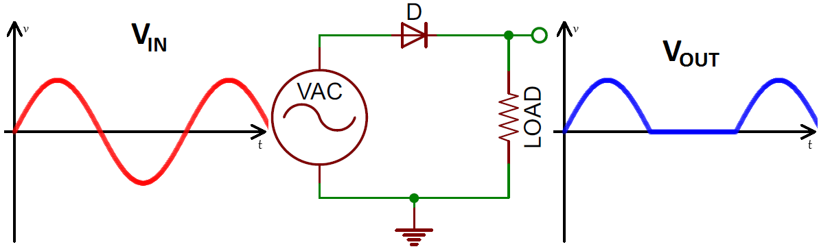
A half-wave rectifier can be made out of just a single diode. If an AC signal, like a sine wave for example, is sent through a diode any negative component to the signal is clipped out.
Half-wave rectifier in/out waveforms and circuit
Input (red/left) and output (blue/right) voltage waveforms, after passing through the half-wave rectifier circuit (middle).
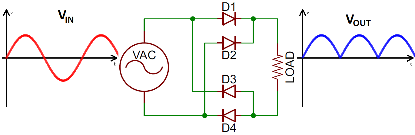
A full-wave bridge rectifier uses four diodes to convert those negative humps in the AC signal into positive humps.
Full-wave bridge rectifier in/out waveforms and circuit
The bridge rectifier circuit (middle), and the output wave form it creates (blue/right).
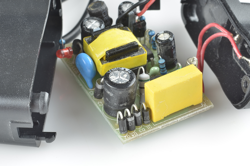
These circuits are a critical component in AC-to-DC power supplies, which turn the wall outlet’s 120/240VAC signal into 3.3V, 5V, 12V, etc. DC signals. If you tore apart a wall-wart, you’d most likely see a handful of diodes in there, rectifying it up.
Diodes in a wall-wart
Can you spot the four diodes making a bridge rectifier in this wall-wart?

Reverse Current Protection

Ever stick a battery in the wrong way? Or switch up the red and black power wires? If so, a diode might be to thank for your circuit still being alive. A diode placed in series with the positive side of the power supply is called a reverse protection diode. It ensures that current can only flow in the positive direction, and the power supply only applies a positive voltage to your circuit.
Reverse current protection circuit
This diode application is useful when a power supply connector isn’t polarized, making it easy to mess up and accidentally connect the negative supply to the positive of the input circuit.
The drawback of a reverse protection diode is that it’ll induce some voltage loss because of the forward voltage drop. This makes Schottky diodes an excellent choice for reverse protection diodes.

Logic Gates

Forget transistors! Simple digital logic gates, like the AND or the OR, can be built out of diodes.
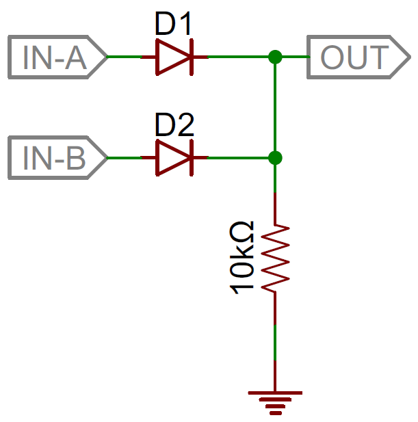
For example, a diode two-input OR gate can be constructed out of two diodes with shared cathode nodes. The output of the logic circuit is also located at that node. Whenever either input (or both) is a logic 1 (high/5V) the output becomes a logic 1 as well. When both inputs are a logic 0 (low/0V), the output is pulled low through the resistor.
Diode 2-input OR gate schematic
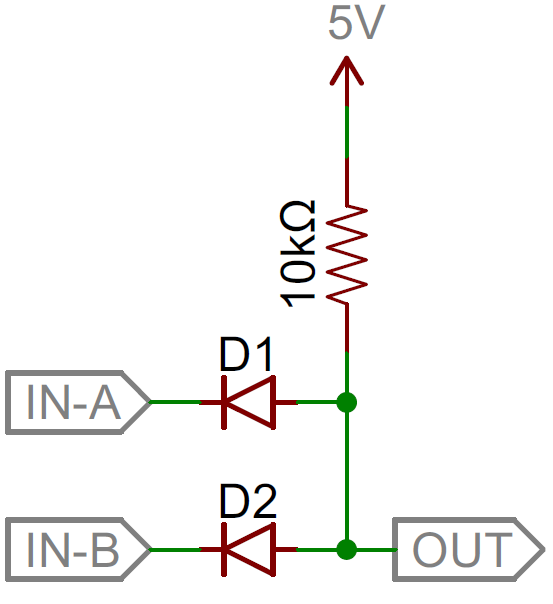
An AND gate is constructed in a similar manner. The anodes of both diodes are connected together, which is where the output of the circuit is located. Both inputs must be logic 1 forcing current to run towards the output pin and pull it high also. If either of the inputs are low, current from the 5V supply runs through the diode.
Diode 2-input AND gate schematic
For both logic gates, more inputs can be added by adding just a single diode.

Flyback Diodes and Voltage Spike Suppression

Diodes are very often used to limit potential damage from unexpected large spikes in voltage. Transient-voltage-suppression (TVS) diodes are specialty diodes, kind of like zener diodes – lowish breakdown voltages (often around 20V) – but with very large power ratings (often in the range of kilowatts). They’re designed to shunt currents and absorb energy when voltages exceed their breakdown voltage.
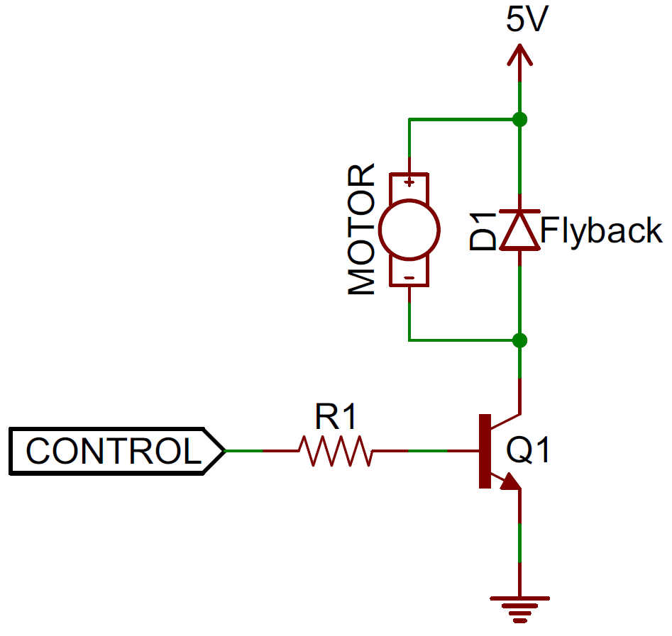
Flyback diodes do a similar job of suppressing voltage spikes, specifically those induced by an inductive component, like a motor. When current through an inductor suddenly changes, a voltage spike is created, possibly a very large, negative spike. A flyback diode placed across the inductive load, will give that negative voltage signal a safe path to discharge, actually looping over-and-over through the inductor and diode until it eventually dies out.
Flyback diode circuit

Introduction

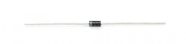
Once you graduate from the simple, passive components that are resistors, capacitors, and inductors, it’s time to step on up to the wonderful world of semiconductors. One of the most widely used semiconductor components is the diode.
alt text
In this tutorial we’ll cover:
  • What is a diode!?
  • Theory of diode operation
  • Important diode properties
  • Different types of diodes
  • What diodes look like
  • Typical diode applications

Ideal Diodes

The key function of an ideal diode is to control the direction of current-flow. Current passing through a diode can only go in one direction, called the forward direction. Current trying to flow the reverse direction is blocked. They’re like the one-way valve of electronics.
If the voltage across a diode is negative, no current can flow*, and the ideal diode looks like an open circuit. In such a situation, the diode is said to be off or reverse biased.
As long as the voltage across the diode isn’t negative, it’ll “turn on” and conduct current. Ideally* a diode would act like a short circuit (0V across it) if it was conducting current. When a diode is conducting current it’s forward biased (electronics jargon for “on”).
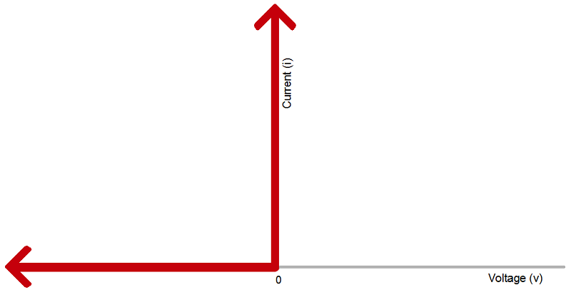
Ideal diode graph
The current-voltage relationship of an ideal diode. Any negative voltage produces zero current – an open circuit. As long as the voltage is non-negative the diode looks like a short circuit.

Ideal Diode Characteristics
Operation ModeOn (Forward biased)Off (Reverse biased)
Current ThroughI>0I=0
Voltage AcrossV=0V<0
Diode looks likeShort circuitOpen circuit

Circuit Symbol

Every diode has two terminals – connections on each end of the component – and those terminals are polarized, meaning the two terminals are distinctly different. It’s important not to mix the connections on a diode up. The positive end of a diode is called the anode, and the negative end is called the cathode. Current can flow from the anode end to the cathode, but not the other direction. If you forget which way current flows through a diode, try to remember the mnemonic ACID: “anode current in diode” (also anode cathode is diode).
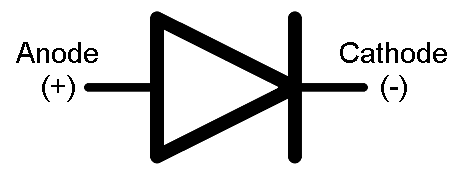
The circuit symbol of a standard diode is a triangle butting up against a line. As we’ll cover in the later in this tutorial, there are a variety of diode types, but usually their circuit symbol will look something like this:
Diode circuit symbol
The terminal entering the flat edge of the triangle represents the anode. Current flows in the direction that the triangle/arrow is pointing, but it can’t go the other way.
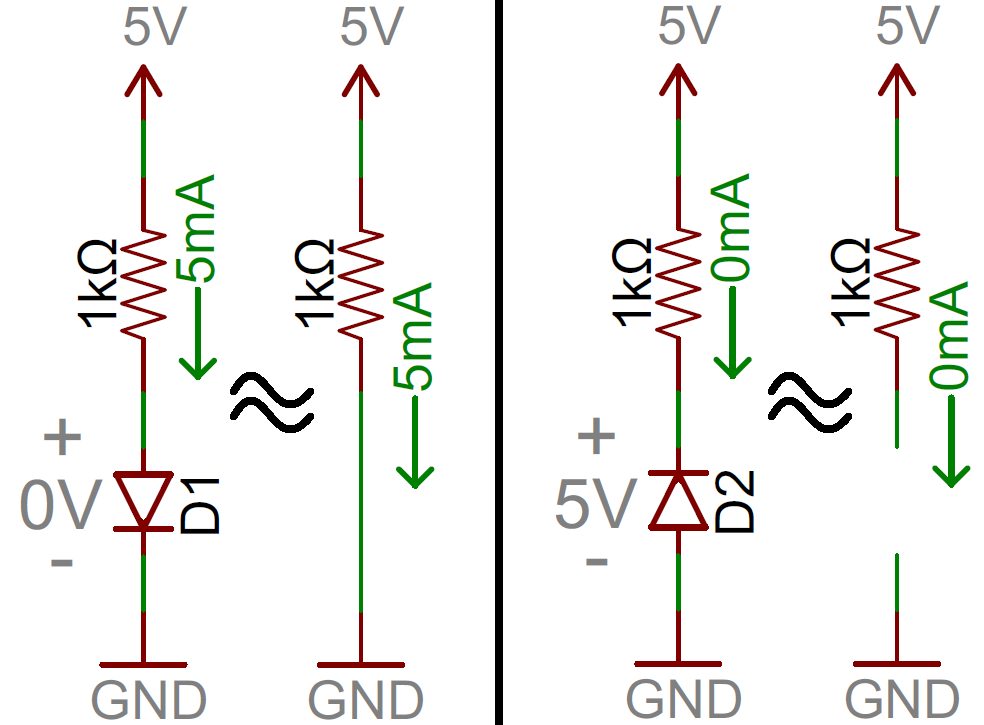
Examples of ideal diodes in circuits
Above are a couple simple diode circuit examples. On the left, diode D1 is forward biased and allowing current to flow through the circuit. In essence it looks like a short circuit. On the right, diode D2 is reverse biased. Current cannot flow through the circuit, and it essentially looks like an open circuit.

*Caveat! Asterisk! Not-entirely-true… Unfortunately, there’s no such thing as an ideal diode. But don’t worry! Diodes really are real, they’ve just got a few characteristics which make them operate as a little less than our ideal model…

Real Diode Characteristics

Ideally, diodes will block any and all current flowing the reverse direction, or just act like a short-circuit if current flow is forward. Unfortunately, actual diode behavior isn’t quite ideal. Diodes do consume some amount of power when conducting forward current, and they won’t block out all reverse current. Real-world diodes are a bit more complicated, and they all have unique characteristics which define how they actually operate.

Current-Voltage Relationship

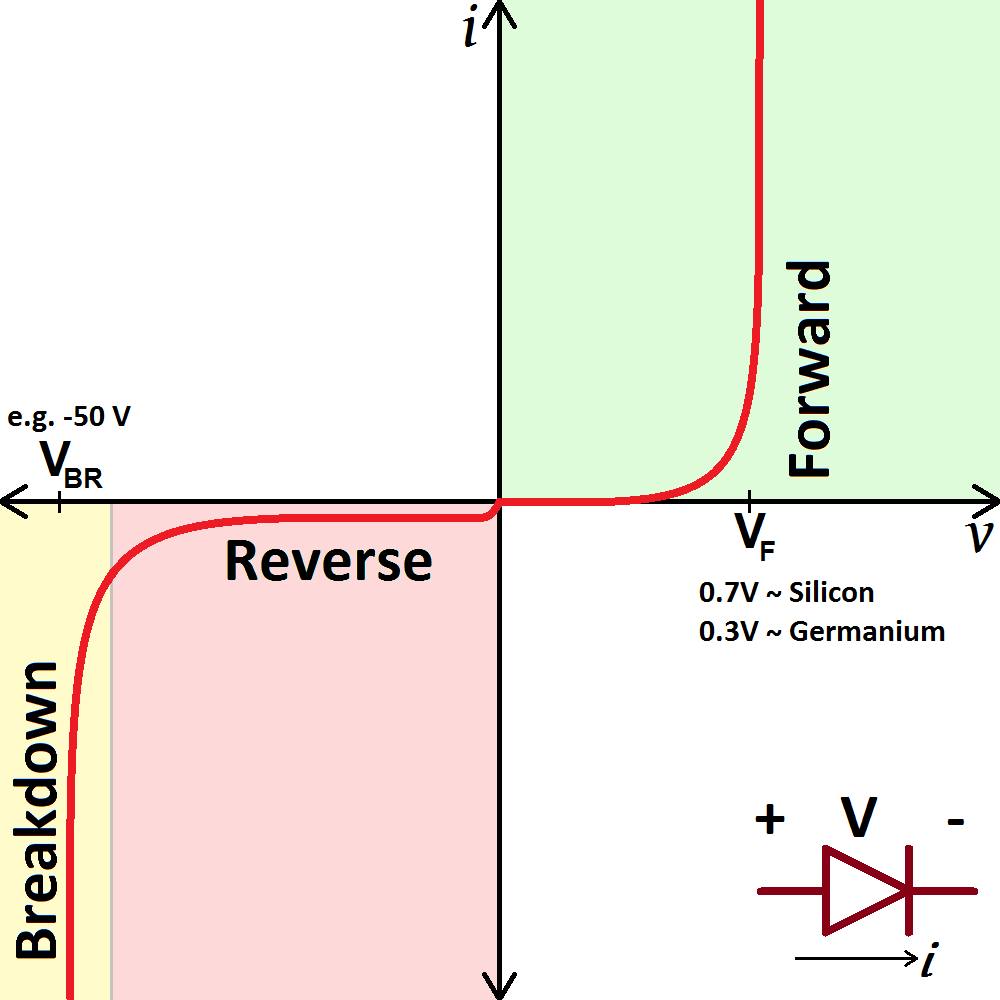
The most important diode characteristic is its current-voltage (i-v) relationship. This defines what the current running through a component is, given what voltage is measured across it. Resistors, for example, have a simple, linear i-v relationship…Ohm’s Law. The i-v curve of a diode, though, is entirely non-linear. It looks something like this:
Real diode i-v curve
The current-voltage relationship of a diode. In order to exaggerate a few important points on the plot, the scales in both the positive and negative halves are not equal.
Depending on the voltage applied across it, a diode will operate in one of three regions:
  1. Forward bias: When the voltage across the diode is positive the diode is “on” and current can run through. The voltage should be greater than the forward voltage (VF) in order for the current to be anything significant.
  2. Reverse bias: This is the “off” mode of the diode, where the voltage is less than VF but greater than -VBR. In this mode current flow is (mostly) blocked, and the diode is off. A very small amount of current (on the order of nA) – called reverse saturation current – is able to flow in reverse through the diode.
  3. Breakdown: When the voltage applied across the diode is very large and negative, lots of current will be able to flow in the reverse direction, from cathode to anode.

Forward Voltage

In order to “turn on” and conduct current in the forward direction, a diode requires a certain amount of positive voltage to be applied across it. The typical voltage required to turn the diode on is called the forward voltage (VF). It might also be called either the cut-in voltage or on-voltage.
As we know from the i-v curve, the current through and voltage across a diode are interdependent. More current means more voltage, less voltage means less current. Once the voltage gets to about the forward voltage rating, though, large increases in current should still only mean a very small increase in voltage. If a diode is fully conducting, it can usually be assumed that the voltage across it is the forward voltage rating.
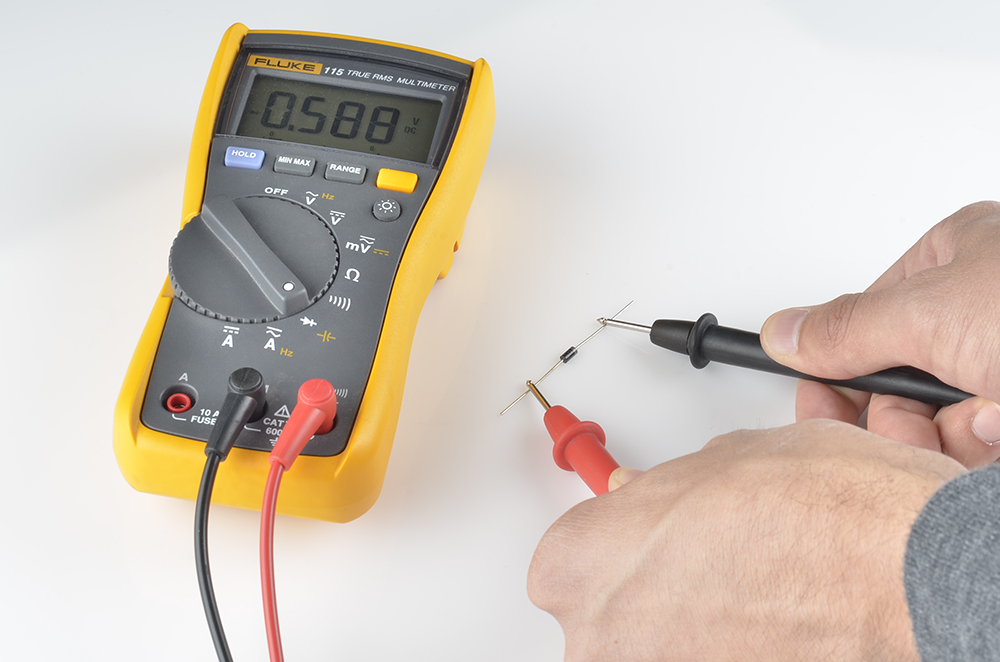
Measuring forward voltage drop
A multimeter with a diode setting can be used to measure (the minimum of) a diode’s forward voltage drop.
A specific diode’s VF depends on what semiconductor material it’s made out of. Typically, a silicon diode will have a VF around 0.6-1V. A germanium-based diode might be lower, around 0.3V. The type of diode also has some importance in defining the forward voltage drop; light-emitting diodes can have a much larger VF, while Schottky diodes are designed specifically to have a much lower-than-usual forward voltage.

Breakdown Voltage

If a large enough negative voltage is applied to the diode, it will give in and allow current to flow in the reverse direction. This large negative voltage is called the breakdown voltage. Some diodes are actually designed to operate in the breakdown region, but for most normal diodes it’s not very healthy for them to be subjected to large negative voltages.
For normal diodes this breakdown voltage is around -50V to -100V, or even more negative.

Diode Datasheets

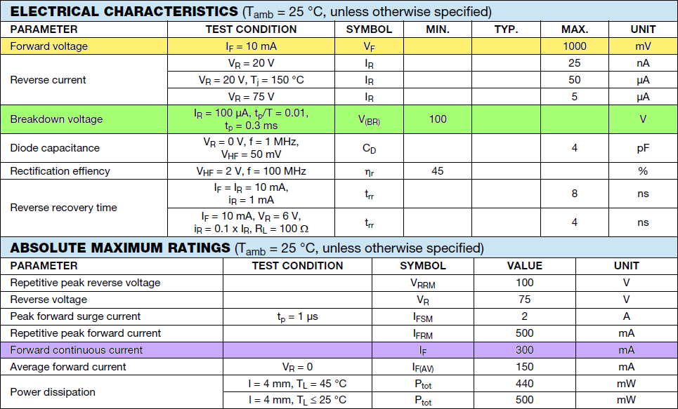
All of the above characteristics should be detailed in the datasheet for every diode. For example, this datasheet for a 1N4148 diode lists the maximum forward voltage (1V) and the breakdown voltage (100V) (among a lot of other information):
1N4148 Datasheet Clipping
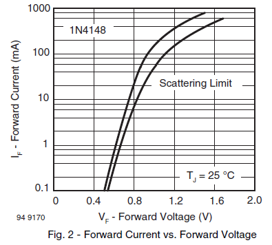
A datasheet might even present you with a very familiar looking current-voltage graph, to further detail how the diode behaves. This graph from the diode’s datasheet enlarges the curvy, forward-region part of the i-v curve. Notice how more current requires more voltage:
1N4148 forward i-v curve
That chart points out another important diode characteristic – the maximum forward current. Just like any component, diodes can only dissipate so much power before they blow. All diodes should list maximum current, reverse voltage, and power dissipation. If a diode is subject to more voltage or current than it can handle, expect it to heat up (or worse; melt, smoke,…).
Some diodes are well-suited to high currents – 1A or more – others like the 1N4148 small-signal diode shown above may only be suited for around 200mA.

That 1N4148 is just a tiny sampling of all the different kinds of diodes there are out there. Next we’ll explore what an amazing variety of diodes there are and what purpose each type serves.

Introduction

These oscillator modules in Learnabout Electronics describe how many commonly used oscillators work, using discrete components and in integrated circuit form. Also learn how to build and test oscillators circuits yourself.

What is an Oscillator

An oscillator provides a source of repetitive A.C. signal across its output terminals without needing any input (except a D.C. supply). The signal generated by the oscillator is usually of constant amplitude.
The wave shape and amplitude are determined by the design of the oscillator circuit and choice of component values.
The frequency of the output wave may be fixed or variable, depending on the oscillator design.

Types of Oscillator

osc-symbol.gif

Fig. 1.0.1 Oscillator
(AC Source)
Circuit Symbol

Oscillators may be classified by the type of signal they produce.
  • SINE WAVE OSCILLATORS produce a sine wave output.
  • RELAXATION OSCILLATORS and ASTABLE MULTIVIBRATORS produce Square waves and rectangular pulses.
  • SWEEP OSCILLATORS produce sawtooth waves.
Sine wave oscillators can also be classified by frequency, or the type of frequency control they use. RF (radio frequency) oscillators working at frequencies above about 30 to 50kHz use LC (inductors and capacitors) or Crystals to control their frequency. These may also be classified as HF, VHF, and UHF oscillators, depending on their frequency.
LF (low frequency) oscillators are generally used for generating frequencies below about 30kHz and are usually RC oscillators, as they use resistors and capacitors to control their frequency.
Square wave oscillators such as relaxation and astable oscillators may be used at any frequency from less than 1Hz up to several GHz and are very often implemented in integrated circuit form.

Sine Wave Oscillators.

Freq-Control-Networks.gif

Fig. 1.0.2 Frequency Control Networks

These circuits ideally produce a pure sine wave output having a constant amplitude and stable frequency. The type of circuit used depends on a number of factors, including the frequency required. Designs based on LC resonant circuits or on crystal resonators are used for ultrasonic and radio frequency applications, but at audio and very low frequencies the physical size of the resonating components, L and C would be too big to be practical.
For this reason a combination of R and C is used to a control frequency. The circuit symbols used for these frequency control networks are shown in Fig. 1.0.2

LC oscillators

radio-tuning-dial.jpg
Inductors and capacitors are combined in a resonating circuit that produces a very good shape of sine wave and has quite good frequency stability. That is, the frequency does not alter very much for changes in the D.C. supply voltage or in ambient temperature, but it is relatively simple, by using variable inductors or capacitors, to make a variable frequency (tuneable) oscillator. LC oscillators are extensively used in generating and receiving RF signals where a variable frequency is required.

RC (or CR) oscillators

Function-Gen.jpg
At low frequencies such as audio the values of L and C needed to produce a resonating circuit would be too large and bulky to be practical. Therefore resistors and capacitors are used in RC filter type combinations to generate sine waves at these frequencies, however it is more difficult to produce a pure sine wave shape using R and C. These low frequency sine wave oscillators are used in many audio applications and different designs are used having either a fixed or variable frequency.

Crystal oscillators

clock-osc.jpg
At radio frequencies and higher, whenever a fixed frequency with very high degree of frequency stability is needed, the component that determines the frequency of oscillation is usually a quartz crystal, which when subjected to an alternating voltage, vibrates at a very precise frequency. The frequency depends on the physical dimensions of the crystal, therefore once the crystal has been manufactured to specific dimensions, the frequency of oscillation is extremely accurate. Crystal oscillator designs can produce either sine wave or square wave signals, and as well as being used to generate very accurate frequency carrier waves in radio transmitters, they also form the basis of the very accurate timing elements in clocks, watches, and computer systems.

Relaxation oscillators

crossing-lights02.gif
These oscillators work on a different principle to sine wave oscillators. They produce a square wave or pulsed output and generally use two amplifiers, and a frequency control network that simply produces a timing delay between two actions. The two amplifiers operate in switch mode, switching fully on or fully off alternately, and as the time, during which the transistors are actually switching, only lasts for a very small fraction of each cycle of the wave, the rest of the cycle they "relax" while the timing network produces the remainder of the wave. An alternative name for this type of oscillator is an "astable multivibrator", this name comes from the fact that they contain more than one oscillating element. There are basically two oscillators, i.e. ''vibrators'', each feeding part of its signal back to the other, and the output changes from a high to a low state and back again continually, i.e. it has no stable state, hence it is astable. Relaxation oscillators can be built using several different designs and can work at many different frequencies. Astables may typically be chosen for such tasks as producing high frequency digital signals. They are also used to produce the relatively low frequency on-off signals for flashing lights.

Sweep oscillators

sweep.jpg
A sweep waveform is another name for a saw-tooth wave. This has a linearly changing (e.g increasing) voltage for almost the whole of one cycle followed by a fast return to the wave’s original value. This wave shape is useful for changing (sweeping) the frequency of a voltage-controlled oscillator, which is an oscillator that can have its frequency varied over a set range by having a variable ‘sweep’ voltage applied to its control input. Sweep oscillators often consist of a ramp generator that is basically a capacitor charged by a constant value of current. Keeping the charging current constant whilst the charging voltage increases, causes the capacitor to charge in a linear fashion rather than its normal exponential curve. At a given point the capacitor is rapidly discharged to return the signal voltage to its original value. These two sections of a saw-tooth wave cycle are called the sweep and the fly-back.
Subscribe to RSS Feed Follow me on Twitter!